
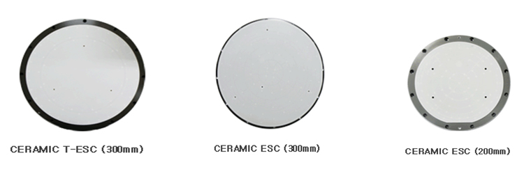
Ceramic ESC
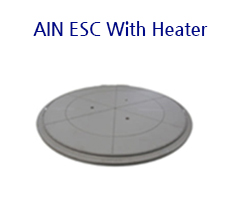
1. AIN ESC with Heater
특징
용도 : 반도체 / PVD / etc
크기 : 4'' ~ 12''
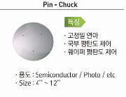
2. Pin - Chuck
특징
용도 : 반도체 / Photo / etc
크기 : 4'' ~ 12''
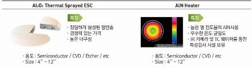
3. AI2O3 THermal Sprayed ESC
특징
용도 : 반도체 / CVD / Etcher /etc
크기 : 4'' ~ 12''
4. AIN Heater
특징
용도 : 반도체 / CVD / etc
크기 : 4'' ~ 12''
ESC의 특징
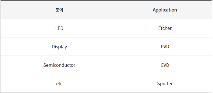
ESC의 분야 및 적용 공정
정전기의 힘을 사용해 기판을 하부 전극에 고정해 주는 핵심 부품. 정전 척(ESC)에 DC 전원('+','-')을 인가시키면 대상물에는 반대의 전위가 대전('-', '+')되고, 대전된 전위에 의하여 서로 끌어당기는 힘이 발생하는 원리
ESC는 정전기적인 힘(Electrostatic force)를 이용하여 반도체 제조 장비 내에서 Wafer를 고정하는 부품으로, 일반적으로 전극의 개수에 따라 Monopolar(Unipolar)와 Bipolar 타입으로 구분되고, 또한 유전층 저항률의 크기에 따라 columb과 Jonsen-Rahb 타입으로 나뉜다.
